webdesigner issues
74HC595
and from Breadboard to PCB
In this tutorial i will show you the way i designed my first PCB from a breadboard layout. The sample consist of 2 74hc595 shift registers
connected together with 16 leds output to a common cathode. The program i use is the latest version of Fritzing
because it's used by a lot of Arduino users, it supports Gerber files and of course ... it's free.
In the youtube video here above you see the sample of the breadboard en the final result on pcb.
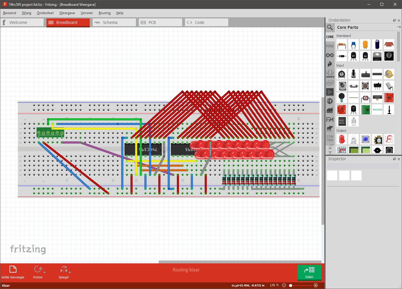 When starting a new project in Fritzing we need only the middle three tabs. We start with the second tab and place our components
from the library on the right panel. There is a community of users making custom compnents on the internet. In this case i place two
74hc595, 16 leds and resistors but leave the Arduino out because i don't want it on the pcb.
When starting a new project in Fritzing we need only the middle three tabs. We start with the second tab and place our components
from the library on the right panel. There is a community of users making custom compnents on the internet. In this case i place two
74hc595, 16 leds and resistors but leave the Arduino out because i don't want it on the pcb.
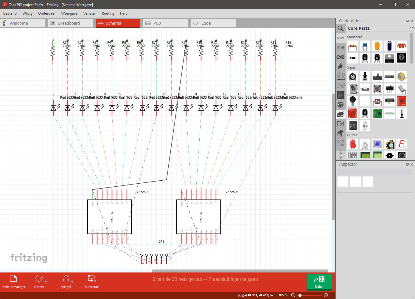 After placing the components on the breadboard you can see a schematic on the third tab. You probably have to re-arrange the components
and checkt the wiring. Scroll out to see al the components and move them together as possible. The schematic can be very disordered and confusing but be cool and
try to re-arrange or rotate the components until the schemtaic become very clearly.
After placing the components on the breadboard you can see a schematic on the third tab. You probably have to re-arrange the components
and checkt the wiring. Scroll out to see al the components and move them together as possible. The schematic can be very disordered and confusing but be cool and
try to re-arrange or rotate the components until the schemtaic become very clearly.
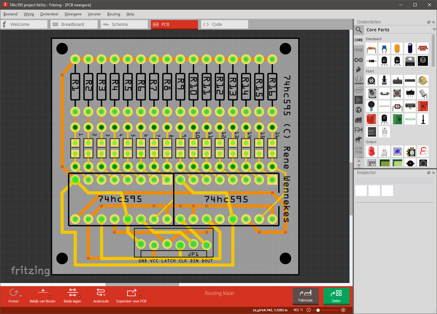 Now the real pcb designing begins. I have to admit that it cost me hours and a some hair becomes gray the first time to made this.
But after a while i figured it out. First bring - like the schematic - all the components together as possible and in the right direction.
In the bottom the program tells you when you're finished with routing (placing the wires on the top or bottom layer). Of course the wires
cannot cross on the same layer. Right-clicking on objects you can alter for example if it will be on the top or bottom layer. Sometimes when you need to go between ic pins,
you can make the lane(s) smaller but always keep in mind for futuring soldering.
Now the real pcb designing begins. I have to admit that it cost me hours and a some hair becomes gray the first time to made this.
But after a while i figured it out. First bring - like the schematic - all the components together as possible and in the right direction.
In the bottom the program tells you when you're finished with routing (placing the wires on the top or bottom layer). Of course the wires
cannot cross on the same layer. Right-clicking on objects you can alter for example if it will be on the top or bottom layer. Sometimes when you need to go between ic pins,
you can make the lane(s) smaller but always keep in mind for futuring soldering.
The design above you will notice something weird about the space for the leds. This is because i had in mind to made this pcb for smd
leds and also for led bar-graphs (like in video).
 When you are really finished - and believe me there is always something you overlooked, if you kown someone who dows the same let your
design checked by him or her, i fortunally i had to control myself - and you're absolutely sure it's perfect, you can export your design
as pdf for printing on sheet ... or, you can export (for production) to rs-274x geber files which i did.
When you are really finished - and believe me there is always something you overlooked, if you kown someone who dows the same let your
design checked by him or her, i fortunally i had to control myself - and you're absolutely sure it's perfect, you can export your design
as pdf for printing on sheet ... or, you can export (for production) to rs-274x geber files which i did.
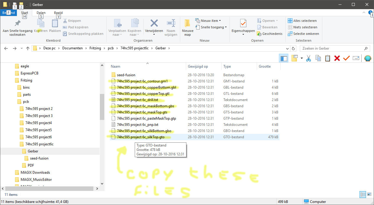
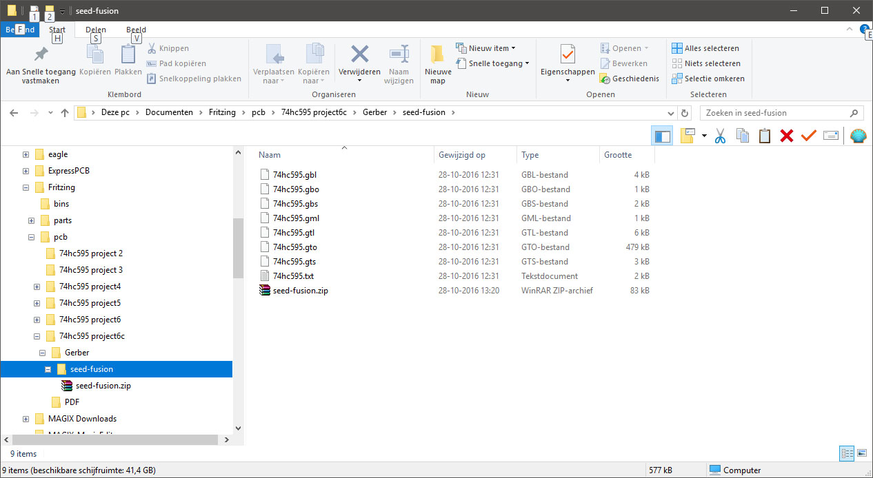 I decided to manufacture my pcb's on Seeedstudio Fusion. On the website
in the FAQ you can find the which files and how they must bu uploaded (zip).
I decided to manufacture my pcb's on Seeedstudio Fusion. On the website
in the FAQ you can find the which files and how they must bu uploaded (zip).
In the pictures (right-click for larger picture) you can see what i had to do to make the correct zip file. In this case the costs for 10 pcb's
of 50x50mm and two layers are 10$ plus 6$ for shipping. Uploading and ready. 2 Weeks later i received my pcb's. I discovered that the holes for
the resistors could be smaller but next time better, right?
I hope you liked this article - if so, like or follow me on youtube - on the bottom you can find the Arduino demo script.
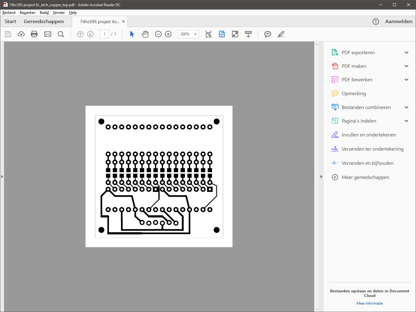 PDF sample for prining on sheets.
shift_74hc595.ino
//**************************************************************//

//  Name    : shiftOutCode, Predefined Dual Array Style         //

//  Author  : Carlyn Maw, Tom Igoe                              //

//  Date    : 25 Oct, 2006                                      //

//  Version : 1.0                                               //

//  Notes   : Code for using a 74HC595 Shift Register           //

//          : to count from 0 to 255                            //

//****************************************************************


//Pin connected to ST_CP of 74HC595

int latchPin = 7;

//Pin connected to SH_CP of 74HC595

int clockPin = 6;

////Pin connected to DS of 74HC595

int dataPin = 5;


//holders for infromation you're going to pass to shifting function

byte segmentArray[10];

unsigned long levelArray[17];


void setup() {

  //set pins to output because they are addressed in the main loop

  pinMode(latchPin, OUTPUT);

  Serial.begin(9600);


  //                  PGFEDCBA

  segmentArray[0] = 0b11000000; //0

  segmentArray[1] = 0b11111001; //1

  segmentArray[2] = 0b10100100; //2

  segmentArray[3] = 0b10110000; //3

  segmentArray[4] = 0b10011001; //4

  segmentArray[5] = 0b10010010; //5

  segmentArray[6] = 0b10000010; //6

  segmentArray[7] = 0b11111000; //7

  segmentArray[8] = 0b10000000; //8

  segmentArray[9] = 0b10010000; //9


  levelArray[0]=  0b0000000000000000;

  levelArray[1]=  0b1000000000000000;

  levelArray[2]=  0b1100000000000000;

  levelArray[3]=  0b1110000000000000;

  levelArray[4]=  0b1111000000000000;

  levelArray[5]=  0b1111100000000000;

  levelArray[6]=  0b1111110000000000;

  levelArray[7]=  0b1111111000000000;

  levelArray[8]=  0b1111111100000000;

  levelArray[9]=  0b1111111110000000;

  levelArray[10]= 0b1111111111000000;

  levelArray[11]= 0b1111111111100000;

  levelArray[12]= 0b1111111111110000;

  levelArray[13]= 0b1111111111111000;

  levelArray[14]= 0b1111111111111100;

  levelArray[15]= 0b1111111111111110;

  levelArray[16]= 0b1111111111111111;


  //function that blinks all the LEDs

  //gets passed the number of blinks and the pause time

  blinkAll_2Bytes(2,500);

}


void loop() {

  for (int i = 0; i < 17; i++) {

    unsigned long j = levelArray[i];

    //load the light sequence you want from array

    //ground latchPin and hold low for as long as you are transmitting

    digitalWrite(latchPin, 0);

    //move 'em out

    shiftOut(dataPin, clockPin, lowByte(j));

    shiftOut(dataPin, clockPin, highByte(j));

    //return the latch pin high to signal chip that it

    //no longer needs to listen for information

    digitalWrite(latchPin, 1);

    delay(100);

  }

  delay(2000);


  /*

  for (unsigned long j = 0; j < 65536; j++) {

    //load the light sequence you want from array

    //ground latchPin and hold low for as long as you are transmitting

    digitalWrite(latchPin, 0);

    //move 'em out

    shiftOut(dataPin, clockPin, lowByte(j));

    shiftOut(dataPin, clockPin, highByte(j));

    //return the latch pin high to signal chip that it

    //no longer needs to listen for information

    digitalWrite(latchPin, 1);

    delay(5);

  }

  */

}


// the heart of the program

void shiftOut(int myDataPin, int myClockPin, byte myDataOut) {

  // This shifts 8 bits out MSB first,

  //on the rising edge of the clock,

  //clock idles low


  //internal function setup

  int i=0;

  int pinState;

  pinMode(myClockPin, OUTPUT);

  pinMode(myDataPin, OUTPUT);


  //clear everything out just in case to

  //prepare shift register for bit shifting

  digitalWrite(myDataPin, 0);

  digitalWrite(myClockPin, 0);


  //for each bit in the byte myDataOutᅵ

  //NOTICE THAT WE ARE COUNTING DOWN in our for loop

  //This means that %00000001 or "1" will go through such

  //that it will be pin Q0 that lights.

  for (i=7; i>=0; i--)  {

    digitalWrite(myClockPin, 0);


    //if the value passed to myDataOut and a bitmask result

    // true then... so if we are at i=6 and our value is

    // %11010100 it would the code compares it to %01000000

    // and proceeds to set pinState to 1.

    pinState= bitRead(myDataOut,i);


    //Sets the pin to HIGH or LOW depending on pinState

    digitalWrite(myDataPin, pinState);

    //register shifts bits on upstroke of clock pin

    digitalWrite(myClockPin, 1);

    //zero the data pin after shift to prevent bleed through

    digitalWrite(myDataPin, 0);

  }


  //stop shifting

  digitalWrite(myClockPin, 0);

}


//blinks the whole register based on the number of times you want to

//blink "n" and the pause between them "d"

//starts with a moment of darkness to make sure the first blink

//has its full visual effect.

void blinkAll_2Bytes(int n, int d) {

  digitalWrite(latchPin, 0);

  shiftOut(dataPin, clockPin, 0);

  shiftOut(dataPin, clockPin, 0);

  digitalWrite(latchPin, 1);

  delay(200);

  for (int x = 0; x < n; x++) {

    digitalWrite(latchPin, 0);

    shiftOut(dataPin, clockPin, 255);

    shiftOut(dataPin, clockPin, 255);

    digitalWrite(latchPin, 1);

    delay(d);

    digitalWrite(latchPin, 0);

    shiftOut(dataPin, clockPin, 0);

    shiftOut(dataPin, clockPin, 0);

    digitalWrite(latchPin, 1);

    delay(d);

  }

}
|
Credits Disclaimer, Contact Sitemap Links |
RSS Feeds |
Contributers: René Wennekes |

|
|
Copyright © 2011 René Wennekes Webdesign |
|||